Design and Analyze
Simulation Page - Layout
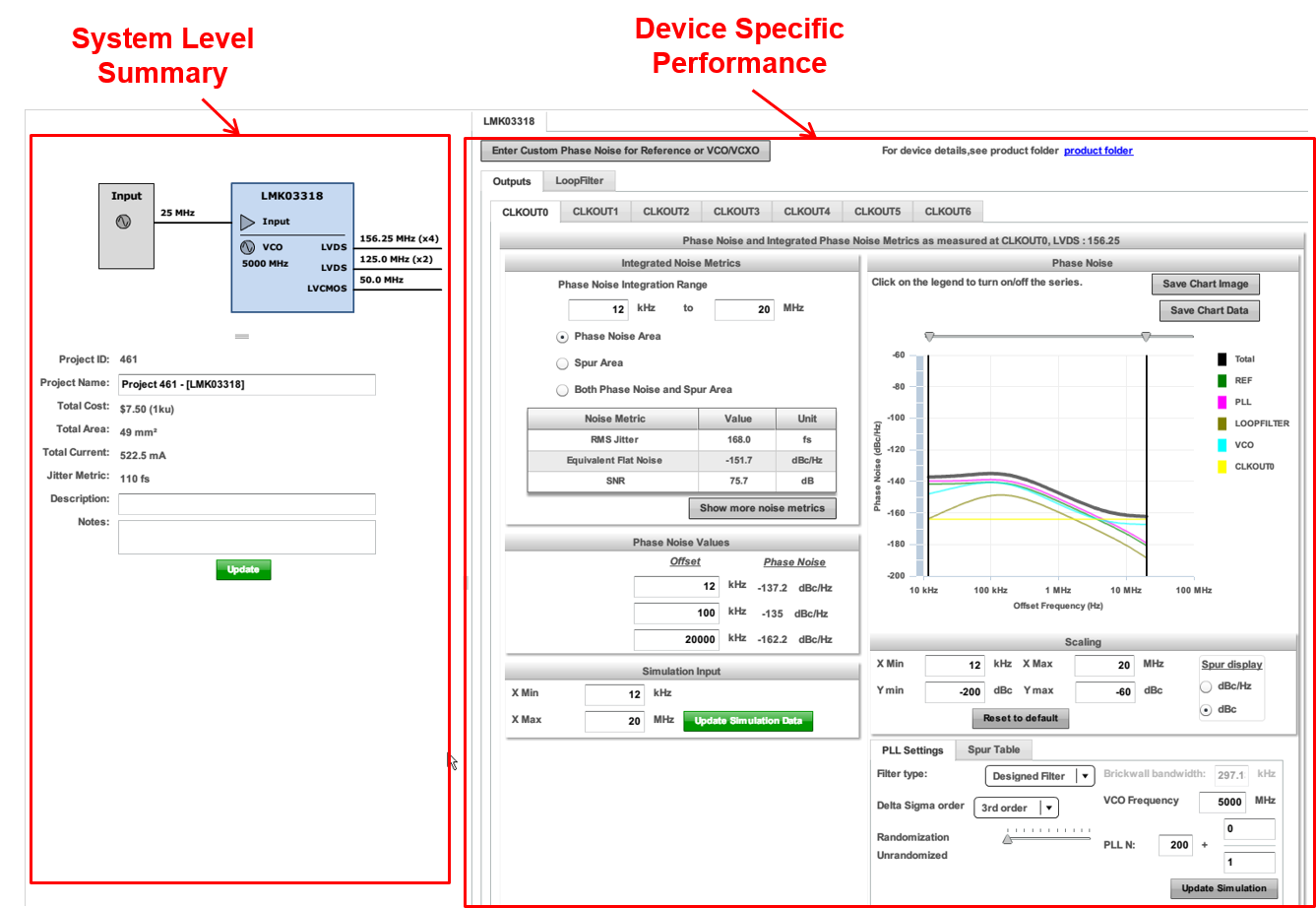
The left side of the simulation page displays a block diagram of the system and summarizes the performance of the system. The right side shows the detailed configuration and simulation results for the selected device. To select a device to configure or simulate, either click on the device in the block diagram or select the device from the top level tab.
Simulation Page - Phase Noise
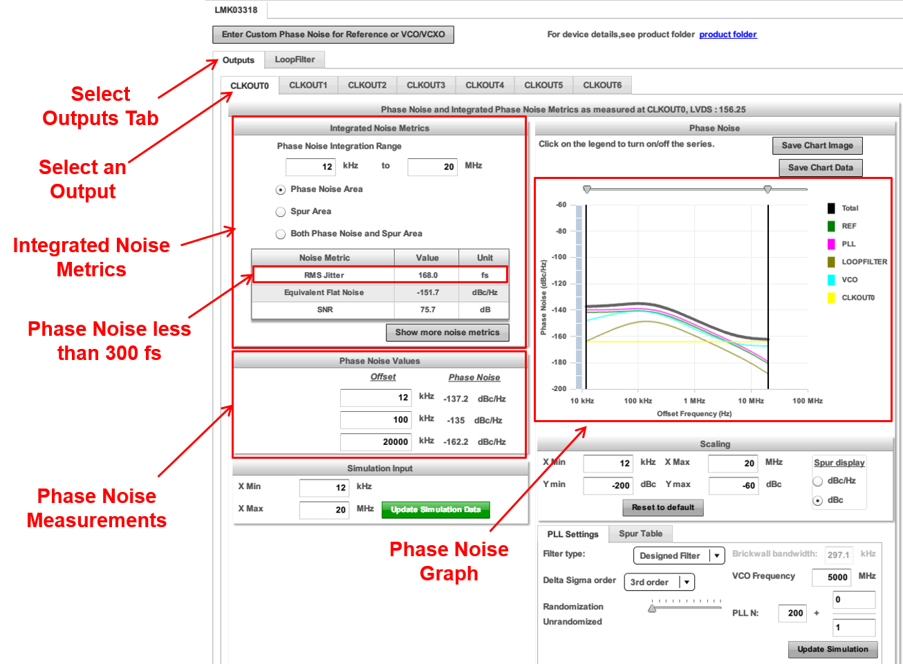
In the simulation page, you can view the phase noise performance for the outputs of each device. Click on the tab of the device you are interested. Ensure that the Outputs tab is selected. Select the output of the device you are interested in.
In the Phase Noise Values section, specify the offset. The tool will display the Total phase noise at that offset.
A summary of the integrated noise metrics is shown. Additional metrics are available if you click on Show All Integrated Noise Metrics. Note that the requirement on the 156.25 MHz output for a Phase Noise of less than 300 ps has been met. You can check the Phase Noise of the other CLKOUT outputs by clicking on the appropriate tabs to determine that the Phase Noise requirements for the other outputs have been met.
Simulation Page - Increased Frequency Range Showing Spurs
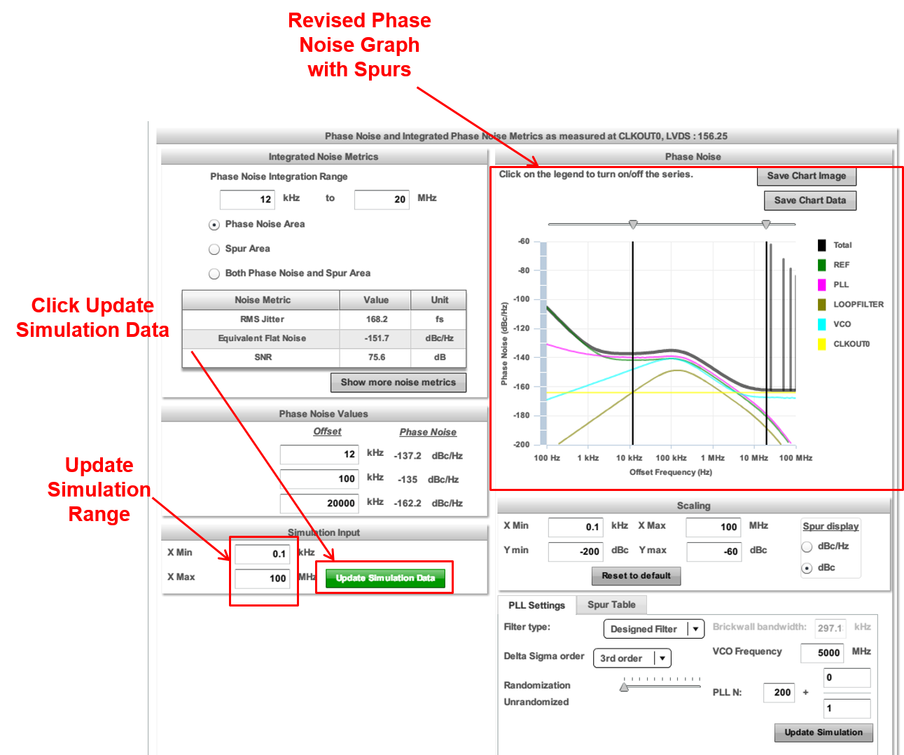
In this example, update the Simulation Input range to a wider range from 0.1 KHz to 100 MHz. Click "Update Simulation Data" and see an expanded range in the Phase Noise graph that shows spurs at the higher frequencies ranges.
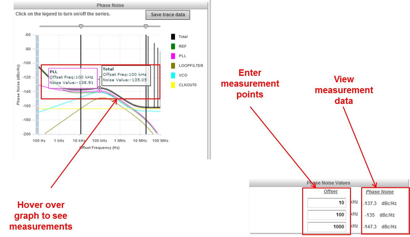
Simulation Page - Phase Noise Measurements
You can measure the Phase Noise by hovering over the graph over manually entering the Phase Noise frequency points in the Phase Noise Values section.
In this example, hover the mouse pointer over that graph to measure total Phase Noise at 100 kHz to be -135 dBc/Hz. Enter the frequencies 10 kHz, 100 kHz, and 1000 kHz in the Phase Noise Values section to measure the total Phase Noise at -137.3 dBc/Hz, -135 dBc/Hz, and -147.3 dBz/Hz respectively.
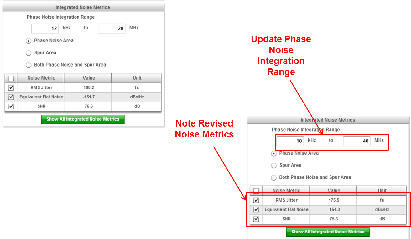
Simulation Page - Phase Noise Integration Range
The Phase Noise Integration Range specifies the frequency range where the Phase Noise and other noise metrics are measured. This may be a subset of the Simulation frequency range.
In this example, widen the Phase Noise Integration Range from 10 kHz to 40 MHz. Note that with a wider integration range, the RMS Jitter increases from 168.2 fs to 175.5 fs. Change the Phase Noise Integration Range back to the default of 12 kHz to 20 MHz.
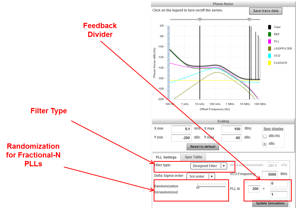
Simulation Page - Phase Noise PLL Settings
In the PLL Settings tab, the Randomization (also known as Dither) and Delta Sigma Order settings apply to a Fractional-N PLL. For Fractional-N PLLs, the PLL N (feedback divider) value consists of an integer and a fractional component.
Filter Type settings can be used to estimate the VCO noise (0 Hz), PLL Flat Noise (Infinite BW) and understand the impact of a Brickwall filter (Brickwall) to the output clock phase noise. The default state of the Filter Type is set to Designed Filter.
In this example, the feedback divider is an integer (200) and does not comprise of a fractional component (fraction numerator =0). Therefore, these parameters can be left alone. The Filter Type is also set to default of Designed Filter. The noise of the Designed Filter is represented in the Phase Noise graph.
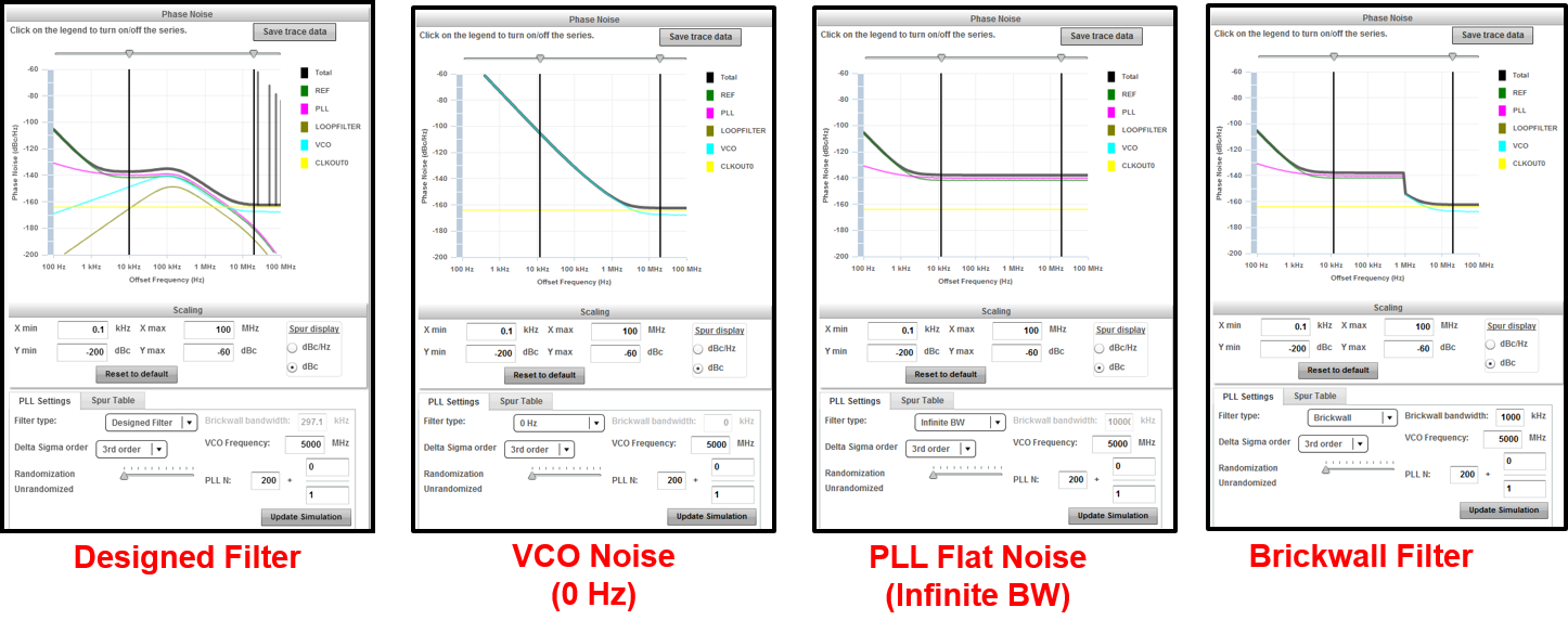
Simulation Page - Phase Noise Filter Type Comparison
In this example, note the different characteristics for Designed Filter, VCO noise (0 Hz), PLL Flat Noise (Infinite BW) and understand the impact of a Brickwall filter (Brickwall) to the output clock phase noise.
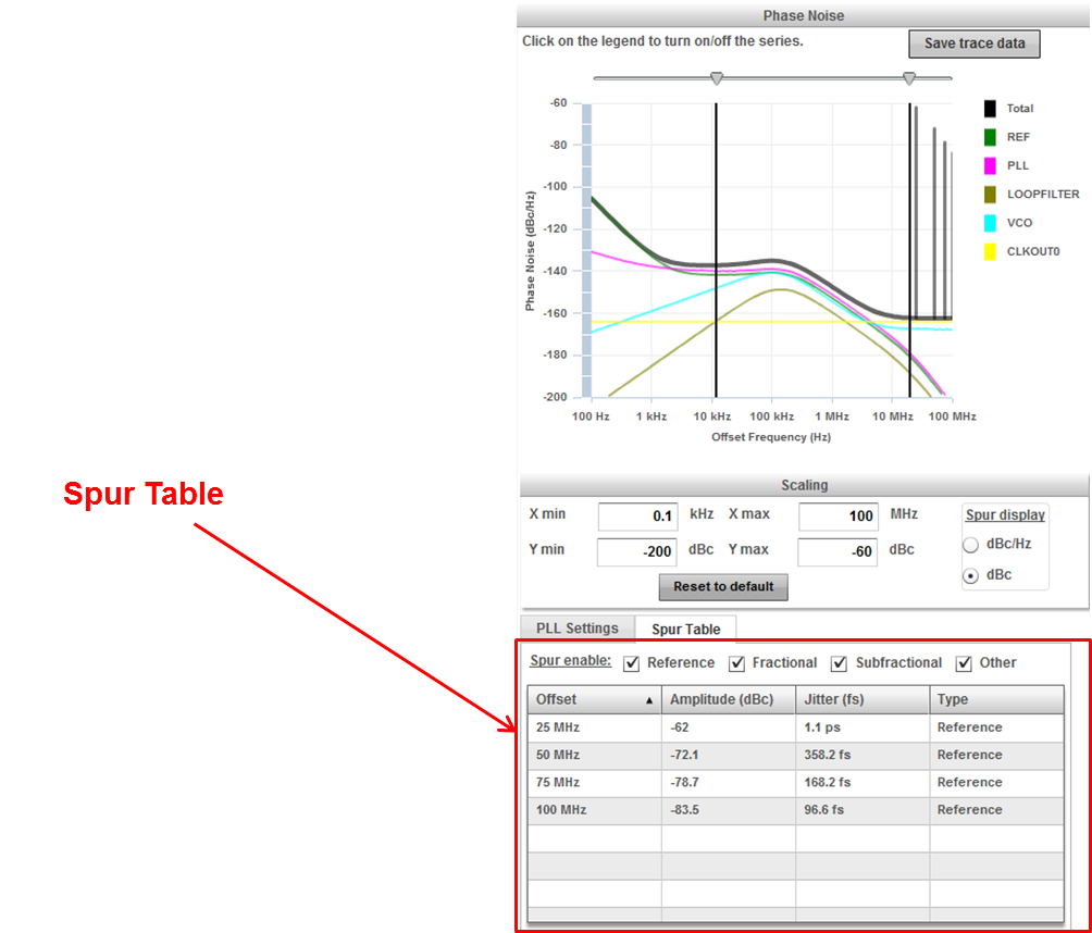
Simulation Page - Phase Noise Spur Table
The output clock phase noise plot includes reference (PFD) spurs. The location of these spurs can be found by clicking on the "Spur Table" tab.
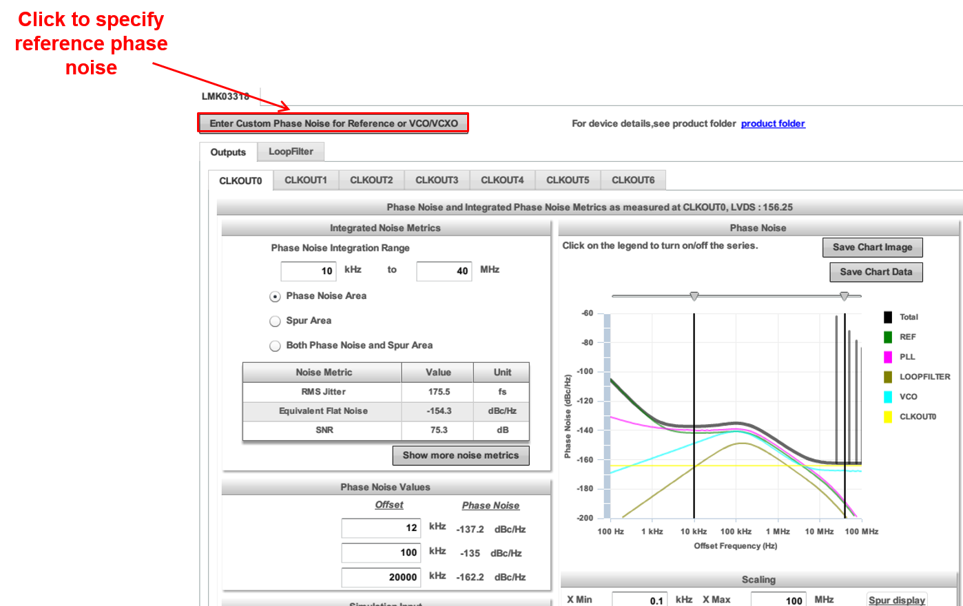
Simulation Page - Reference Custom Phase Noise
You can specify the phase noise of a noisy reference to improve the accuracy of the phase noise simulation and calculation of the integrated noise metrics.
In this example, click on "Enter Customer Phase Noise for Reference or VCO/VCXO" button in order to enter the phase noise data for the 25 MHz reference clock used for generating the desired output frequencies.
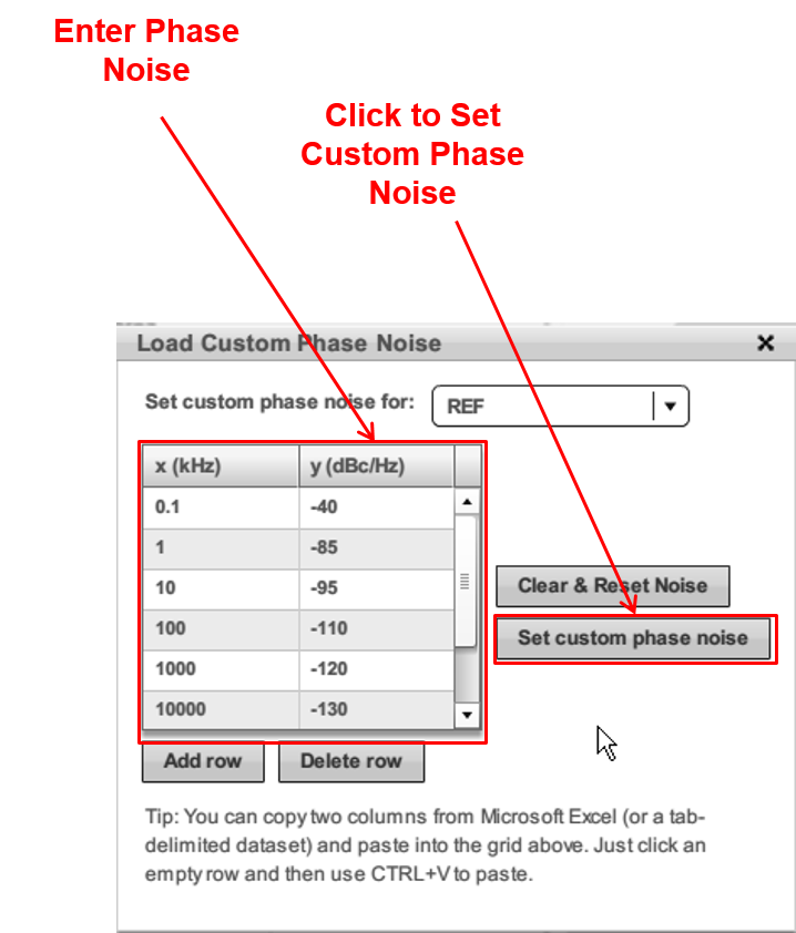
Simulation Page - Reference Custom Phase Noise
Enter the phase noise of a noisy reference clock to be as shown in the example below. Enter the phase noise in dBc/Hz at the various offsets from the carrier and click on "Set custom phase noise".
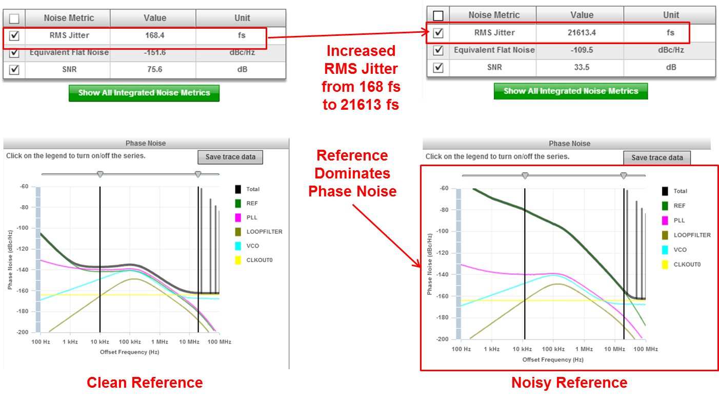
Simulation Page - Effects of Non Ideal Reference
Here is a comparison of the noise metrics and phase noise graph between a clean reference and the noise reference that we just defined. Note that the integrated RMS Jitter increases significantly from 168 fs to 21613.4 fs. Also note that the reference dominates the noise in the Phase Noise graph.
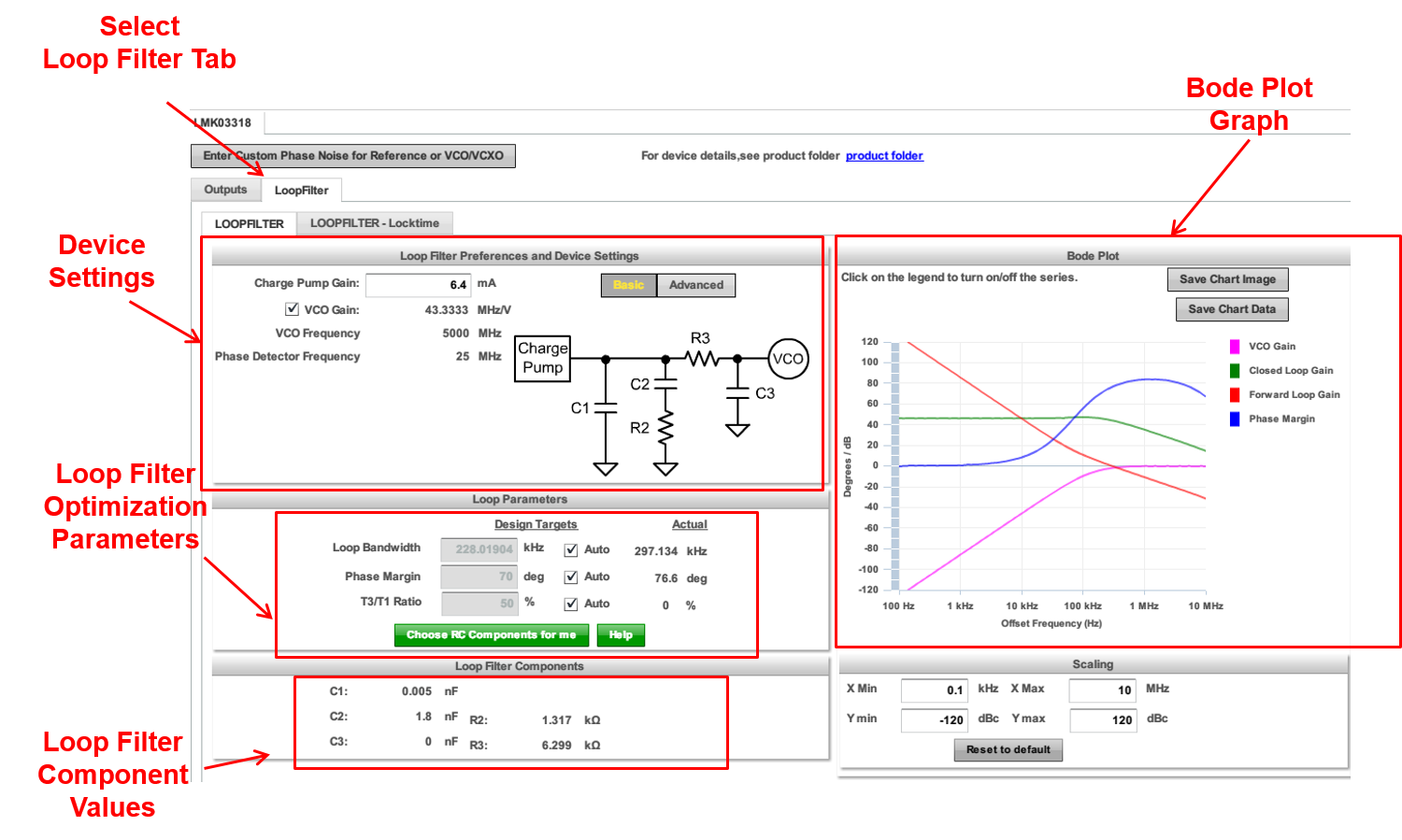
Simulation Page - Loop Filter Configuration
Each device may have one or more loop filters. To configure the loop filter, select the device you want to configure. Click on the LoopFilter tab. Then, select the loop filter that you want to configure.
In the Device Settings section, specify the charge pump gain, VCO gain, VCO frequency, and phase detector frequency.
In the loop filter section, specify performance parameters for your loop filter which includes loop bandwidth, phase margin, and T3/T1 ratio. Click Update to view the recommended component values for your loop filter and an updated Bode Plot graph.
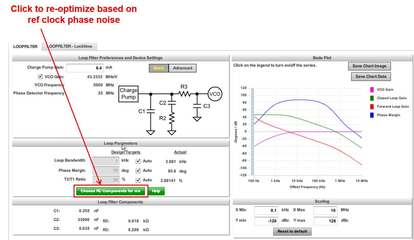
Simulation Page - Updating Loop Filter for Reference Phase Noise
Next we will take a look at the LoopFilter tab to see if we can somehow minimize this integrated jitter.
In this example, it is necessary to click on the "Choose RC Components for m" button in order to re-optimize the loop to minimize the integrated RMS jitter given the updated reference clock phase noise (entered in the table previously). Click OK for the Warning.
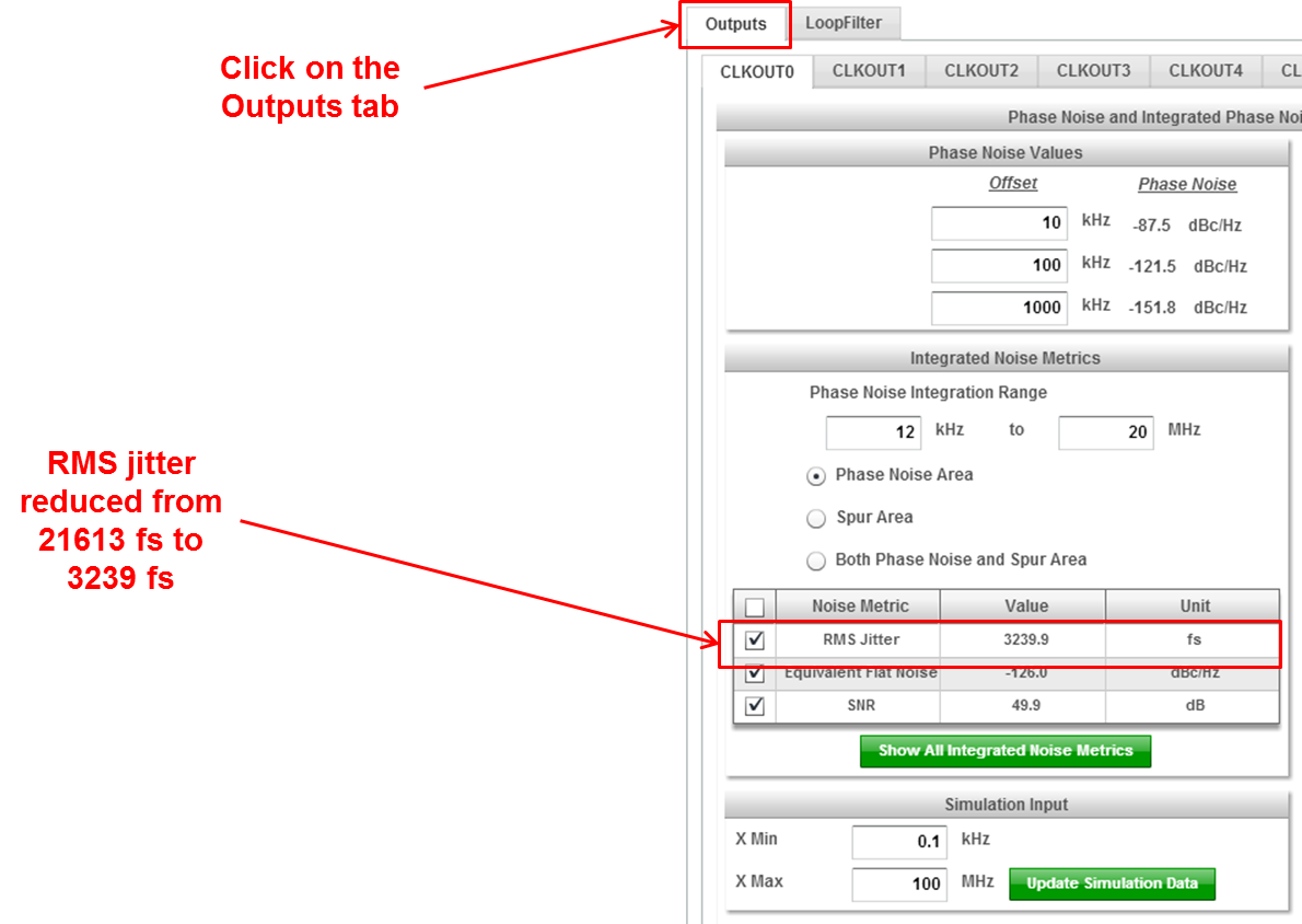
Simulation Page - RMS Jitter after Optimizing Loop Filter
Now, go back to the outputs tab to check the CLKOUT0 156.25 MHz integrated RMS jitter is reduced. Notice that the integrated RMS jitter went down from 21613.4 fs to 3239.9 fs. This is a significant reduction.
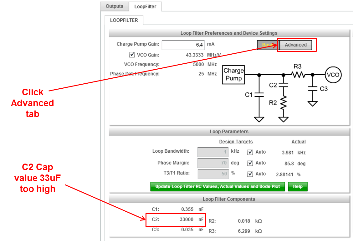
Simulation Page - Optimizing Component Values
Go back to the Loop Filter Tab. Notice in the Loop Filter Components that the value of the C2 capacitor is 33uF! We should try to restrict the value of C2 to be <= 10uF in order to minimize the size of the external filter components.
In order to go about achieving this, click on the Advanced button under Loop Filter Preferences and Device Settings.
Simulation Page - Optimizing Component Values (Cont)
Minimize the charge pump current to its lowest allowable value in the datasheet (0.4mA) and set a lower phase detector rate (5 MHz). Click on "Choose RC Components for me" button once again. Notice that the value of the C2 filter component is now 1.5uF.
Reducing charge pump current increases the PLL in-band (below loop bandwidth) phase noise. Under normal circumstances, it is desirable to set the charge pump current (gain) as high as possible. The other implication of setting a high charge pump current (gain) setting is that the PLL loop bandwidth scales proportionally. In order to clean jitter on the reference clock, it is desirable to have a low PLL loop bandwidth. Therefore the charge pump current should be set to a low value. For cases, where the desired phase noise integration bandwidth falls beyond the PLL loop bandwidth, this tradeoff of minimizing the charge pump current to minimize the PLL loop bandwidth at the expense of higher in-band phase noise is justified.
Setting a low phase detector rate or higher value of the feedback divider (N) reduces the PLL loop bandwidth since PLL loop bandwidth is inversely proportional to feedback divider value. This is another means to achieve lower loop bandwidths
Go back to the outputs tab and notice that the integrated jitter is down less than 1000 fs.

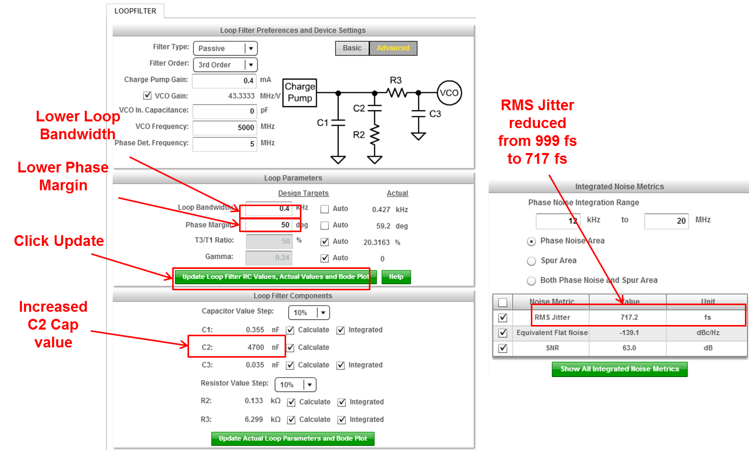
Simulation Page - Further Loop Filter Optimization
To see if we further optimize the jitter, go back to the Loop Filter tab and uncheck the Auto checkbox for Loop Bandwidth and Phase Margin under Design Targets in Loop Parameters section. Set Loop Bandwidth to 0.4kHz (the bandwidth is set lower here intentionally to minimize the contribution due to the dirty reference clock) and Phase Margin to 50 degrees (enables fast roll off after the loop bandwidth). Click on the "Choose RC Components for me" button.
Notice that C2 is <=10uF and Integrated RMS Jitter in the outputs tab is down to 717.2 fs. Further optimization can potentially be achieved but not attempted for the purposes of this demo.
A lower phase margin setting (50 degrees vs. 70 degrees) helps to roll off the Phase noise beyond the loop bandwidth much faster at the expense of some peaking around the loop bandwidth (due to reduced damping factor)
Controlling PLL charge pump current and phase margin therefore helps to minimize the value of the C2 capacitor.