Create or open an existing WEBENCH design
Once the WEBENCH Designer software starts up, use the WEBENCH Visualizer to select an appropriate solution for your needs. You can use the WEBENCH Optimizer dial to tune your design for high efficiency, small footprint or low price. Once you have found the desired solution, click on the Open Design button to create a design in WEBENCH Designer

Edit design
Once the design has been created, you can use all the award winning WEBENCH features to characterize your design. This includes charts and tables of the key operating values, electrical simulation, thermal simulation and design export.
When you have finished characterizing your design, you may want to modify the circuit schematic to include other features or additions such as a ripple filter, RC snubber, additional outputs, board parasitics, etc. To do this, click on the Edit this Design link.

Copy design to edit and simulate
A dialog will appear which allows you to change the name of the design and enter comments. To proceed with the edit process, click on the Edit This Design button. This will create a copy of the original design and you will be editing this copy. This copy no longer has the normal WEBENCH operating features since the topology of the edited design may change from the original. But the original design is preserved and can be accessed through the MyDesigns/Projects link in the upper left of any WEBENCH Designer page.
The new design may be edited using the on line schematic capture tools and simulated using the integrated Spice simulator.

WEBENCH Schematic Editor
This is the WEBENCH schematic editing screen that can be accessed by clicking on the Edit Schematic button in the navigation bar. The main editing toolbar is just above the schematic.
Navigation bar
The WEBENCH navigation bar allows the user to switch between different steps in the WEBENCH Schematic Editor.
Editor Toolbar
The editing toolbar gives the user the ability to do the following:
1) Zoom: Zooms the schematic centered around the current view. This is also accessible from the right click menu.
2) Fit: Zooms to fit the entire schematic into the viewable area.
3) Pan: After clicking the Pan tool, click and drag the schematic to reposition it.
4) Select: After clicking the Select tool, it allows the user to do the following to the schematic:
A) Click and drag the mouse to select an area. Anything touched by the drag box will be selected.
B) Click to select an individual component or wire.
C) Add more to the selection by pressing the control key while clicking on additional components or wires. Can also remove individual items from a selection using this control/click feature.
D) After selecting items, they can be moved by clicking and dragging with the mouse.
5) Rotate: Rotate a selected component. May also be done using the shift r key combination.
6) Delete: Delete selected components and/or wires. May also be done using the delete key.
7) Copy: Copy selected components and/or wires. May also be done using the control c key combination.
8) Cut (not in toolbar): Cut selected components and/or wires using the control x key combination.
9) Paste: Paste copied or cut components and/or wires. May also be done using the control v key combination.
10) Wire: Place wires in the schematic. Click and release to start, click for each vertex and hit escape key to end after the last vertex is placed. May also be started by using the w key.
11) Resistor, capacitor, inductor and diode: Place respective components in the schematic. May also be done using the r, c, l and d keys respectively. A component which is newly placed will have no value so the user must use the select alternate component feature (right click menu) in order to select a component or enter a custom value.
12) Undo: Reverses the last operation.
13) File menu:
A) Save the design. Note that any changes to the schematic are not automatically saved unless the user manually saves, or goes to another page within the WEBENCH Designer application. So remember to save often.
B) Get a PDF design report.
14) Show/Hide menu: Can toggle various indicators and labels on and off within the schematic.
15) Place part / passives: Place a passive component on the schematic

Schematic Editor Toolbar
More options for Place Part include:
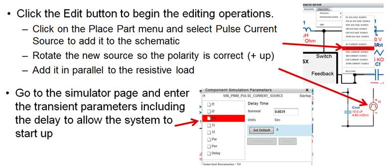
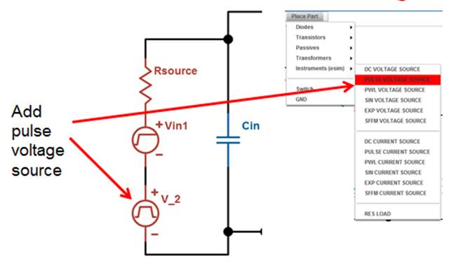
1) Place Part / Instruments (esim): Add a simulation voltage or current source to the schematic. After placement, this can be configured on the simulation page by clicking on the Sim button in the top navigation bar.
2) Place Part / ICs: This menu is not yet enabled.
3) Place Part / GND, GND_Signal, Continuation: Place ground symbols and continuation (port) symbols (not yet enabled).

Right click menus
Right clicking on a component allows the user to perform an operation on the component including, rotate, mirror, delete.
Select Alternate Component takes the user to the select alternate component page.
Right clicking in a blank area of the schematic displays a menu of choices, as well.

Edit schematic - add wire
Add a wire by clicking on the add wire tool or by using the w key. This causes a crosshair to appear. Click and release the mouse to place the first vertex of the wire. Subsequent mouse clicks will place more vertices. End the current wire placement by using the escape key one time. Hitting the escape key twice puts the application back into select mode.

Edit schematic
This diagram shows an LC filter added to an existing schematic.
To rename a component, select it then change the name using the rename box in the upper left. Make sure to click the Rename button to initiate the change.
Next, right click on a component and click on select alternate to go to the component selection screen.

Select component
On the Select Component page, enter the upper bound, lower bound and target for the listed parameters. Then click the search button to get results from the WEBENCH passive component database. Use the Visualizer graph on the left to make tradeoffs between important parameters. Or sort the table on any column to better achieve the desired results. Select the desired component using the Select button. You can also create a custom component by using the Create a Custom Part button at the bottom of the page.

BOM listing
The BOM page lists the entire bill of materials for the design. Click on the Select Alternate Part button next to a component to change it.

Start simulation
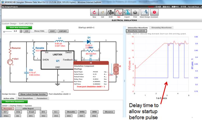
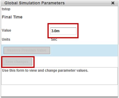
On the simulation page, right click on a simulation source to modify its properties.
Right click on a component to change it, get component properties or zoom in on the component.
Use the zoom controls in the upper left of the schematic or the right click menu to adjust the zoom level.
Move the schematic by clicking and dragging with the mouse.
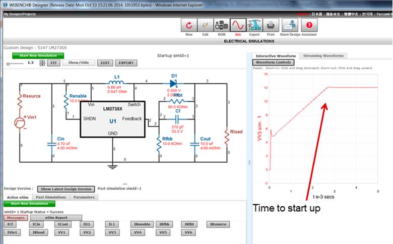
Click the Start New Simulation button to initiate a simulation.

Simulation complete
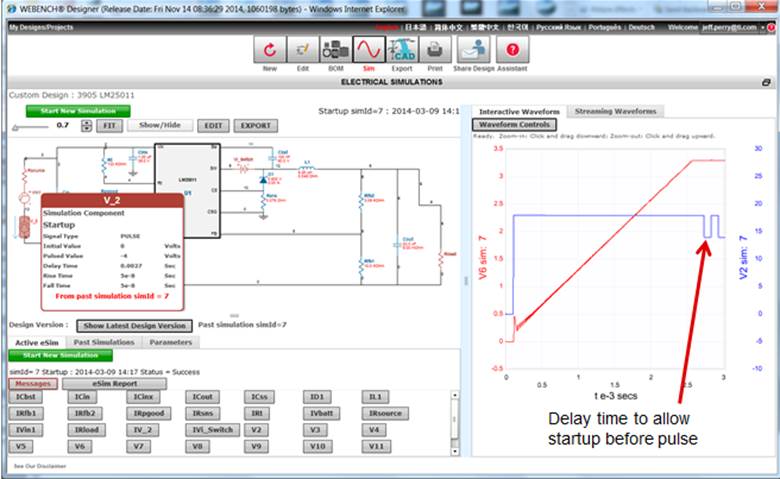
When the simulation is complete, click on a wire or a button in the Active eSim tab to view the waveform for a voltage node.

Click on a component or a button to view the current waveform through that component. The arrow shows the direction of the current. The polarity of a waveform can be reversed in the waveform viewer using the right click menu on the waveform's Y axis.

View waveform
In the waveform viewer, click and drag down and to the right to zoom in. Click and drag up and to the left to reset the zoom.
Right click on one of the y axes to access additional controls.
The advanced waveform controls can be accessed from the Waveform Controls button.

Waveform controls
The advanced waveform controls include the following:
1) On the Loaded waveforms tab there are controls for each waveform to adjust its appearance. Waveforms can be grouped together on a common axis using the Group Voltages or Group Currents buttons.
2) On the Add/Remove Waveforms tab, recall simulations from other designs so they can be overlaid with the current simulation.
3) On the marker tab turn on a pop up indicator which shows the values on the plot at the mouse position.

Sim status and report
On the bottom of the Active eSim tab use the buttons to show messages about the current sim and also to generate a PDF report of the electrical simulation results. Alternatively there is a button to generate the eSim report on the Past Simulations tab. The eSim report documents the schematic, BOM and the waveforms for the current simulation.

Sim status
The Past Simulations tab lists all the past simulations for the design. Click on the View button for a past simulation to activate it. This will display the schematic state when the past simulation was run. Then recall any desired waveforms from that simulation. Get an eSim report for any past sim by clicking on the report button for that sim.
The simulation results in this example show the effect of two different filter inductors. The red waveform is the output voltage before the filter which averages 3.3V at steady state. The blue waveform is the output voltage after the filter using a small filter inductor with an 18 mOhm DC resistance. This causes the output voltage to drop by about 25mV, but the ripple has been reduced substantially. The green waveform shows the output voltage after a filter using a 0.71 mOhm DCR inductor. This shows little or no voltage drop vs the unfiltered output and the ripple is still reduced. However, the inductor is larger.
To restore the current schematic state, click on the Show Latest Design Version button.
You Access you past designs using the My Designs/Projects link in the upper left of the screen.

Schematic export
Export the schematic to popular CAD tools by using the Export feature. Simply select the desired output format, download the file and then load it into the CAD tool.

Print design report
Click on the Print button in the navigation bar to generate a design report. This contains the schematic and bill of materials for the edited design.

Share design
Click on the Share Design button in the upper navigation bar to share the design. Enter the destination email, personal note and specify which simulations to include with the shared design. Click on the green Share This Design button to initiate the process. This will send an email to the destination address inviting the user to click on a link to receive the design. After that, a copy of the design will be put in the new user's workspace.

